NHBR About Town: Week of July 17, 2026
Business and event happenings around the state of NH
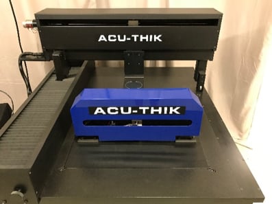
Acu-Gage Systems — a Hudson-based manufacturer of non-contact coordinate measuring machines serving medical, semiconductor, aerospace and other industries — has been awarded a patent for its ACU-THIK precision thickness measuring system.
All 21 patent claims were approved readily by the U.S. Patent and Trademark Office “because there is no other machine available that can match ACU-THIK for thin substrate thickness accuracy across all X, Y coordinates,” said the company in a press release.
ACU-THIK is an automated thickness measurement tool incorporating dual contact probes for high accuracy inspection of semiconductor wafers and other thin substrates. Six Heidenhain measuring devices are integrated into the ACU-THIK system, which can be configured to accommodate wafer diameters of 100 millimeter – 400 mm and larger.
Diagnosing as well as controlling thickness, bow and warp in semiconductor wafer production is now automated when ACU-THIK users preprogram multiple pattern operations to fulfill planned production cycles, said the company. Additionally, the system supports robotics integration to free up operators’ time for other important tasks.
“This is a tremendous breakthrough for Acu-Gage and the semiconductor manufacturing industry as well as some others,” remarked Acu-Gage President Jack Kane in a press release. “Our customers can be confident in implementing the only truly automated and extremely accurate thickness measuring system in the world for their quality control. Some of our customers have known this for a while and having the technology patented now offers us new opportunities.”

Business and event happenings around the state of NH

The Latest is a roundup of the comings and goings of the movers and shakers in NH's business community

A decade after buying the property to redevelop it into a new generation of vacation cabins, the owner of Presidential Mountain Resort LLC (PMR) in Bethlehem has filed for bankruptcy protection in New York’s federal court, claiming more than $13 million in liabilities owed.

Failure to restore ACA tax cuts will only make things worse, according to U.S. Sen. Maggie Hassan

One of the things I enjoy most about working with New Hampshire business owners is hearing what they’re building toward. Whether it’s growth, succession or greater stability, our conversations are almost always about the future.

For many business owners, building wealth is closely tied to the success of the company. But as revenue grows and priorities shift, it can be difficult to know how much cash to keep available, how much to reinvest and when to begin planning for longer-term goals.

Succession planning for your business goes beyond naming the next leader. It involves preserving continuity for your employees and customers, as well as supporting the company’s long-term success.

As we close out Q2 and review the year so far, there are several interesting dynamics at play.

Londonderry’s Town Council is at odds over legal matters pertaining to hiring outside law firms to handle complaints and allegations of misconduct against the town manager.